Enter the market: the Russian lithograph will accelerate the production of microcircuits by 3 thousand times
- Статьи
- Science and technology
- Enter the market: the Russian lithograph will accelerate the production of microcircuits by 3 thousand times


A Russian startup has developed a multipath electronic lithograph project for the production of modern microchips. A key technology has already been created and tested for it — a multicathode that allows the formation of multiple electron beams at once. Thanks to this, the installation will be able to expose a silicon wafer in just 5-7 minutes — approximately 3 thousand times. times faster than traditional single-beam electronic lithographs. The developers expect that the new solution will allow them to compete with their foreign counterparts in the Russian market and strengthen the country's position in the field of microelectronics. At the same time, experts note that the project is still at an early stage of development, so it may take a long time before full-fledged working prototypes appear.
Multipath Electronic Lithograph Project
The Russian team, with the support of the NTI, has created a multipath electronic lithograph project, which, according to the calculations of the developers, is able to reduce the exposure time of a silicon wafer — drawing a pattern on its surface — from one and a half to two weeks to several minutes. The installation is based on a multicathode, a single source that generates multiple electron beams at once instead of one, as in traditional electronic lithographs.
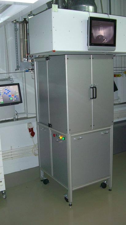
So far, we are not talking about a finished machine, but about the completed stage of scientific research. The lithograph itself is to be created as part of the next stage — development. At the same time, the key element of the system, the multicathode, has already been manufactured and has passed practical tests. For the first time, the lithograph project was presented at the forum "Strong Ideas for Modern Times".
— We have developed an end-to-end technology for creating a multicathode and have confirmed its operability in practice. We have managed to obtain arrays of electron beam sources with a radius of rounded tip of only 1.5–2 nanometers, which is one of the best results in the world. It is this element that allows you to generate multiple electron beams simultaneously and speed up the lithography process many times," Evgeny Givargizov, the main developer of the project, told Izvestia.

According to him, the main advantage of the technology over existing multipath solutions was the way the electronic sources themselves were generated. Unlike foreign systems that use complex single-beam splitting schemes with a large number of mirrors and optical shutters, the Russian development creates many independent electron sources on a single substrate at once. This significantly reduces the requirements for engineering infrastructure, energy consumption, and equipment costs.
The developers expect that when the project is launched, the first prototype lithograph can be created in about three years. In the future, the technology, according to their estimates, will be able to be used for the production of microcircuits with various technological standards — from traditional 350 nm to promising processes with a topology of several nanometers. At the same time, as the project team notes, the maximum resolution today is determined primarily by the characteristics of the photoresists used, and not by the capabilities of the electron beam source itself.

A new lithograph in the development of domestic technologies
According to experts, the concept of multipath electronic lithography itself is indeed capable of becoming an important area for the development of domestic equipment, but the development has a long way to go before industrial implementation.
— The technology looks interesting and promising. If it is possible to reliably implement a multicathode and ensure precise control of a large number of electron beams, this can significantly speed up the exposure process and make production cheaper and more flexible compared to classical single-beam systems. In the long term, such solutions can help Russia develop its own equipment and reduce dependence on imports, but there is still a lot of work to be done before a full—fledged industrial alternative to the world's leading systems," said Sergey Sazonov, NTI expert on microelectronics and the electronics industry.
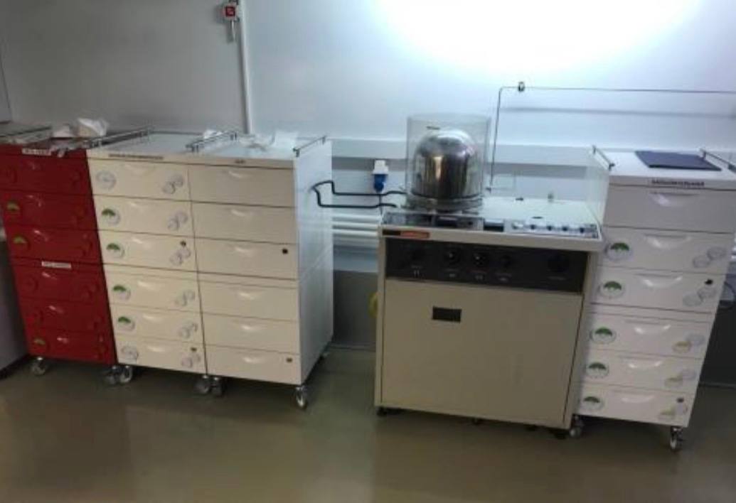
Sergey Varnavsky, a specialist in engineering and technical expertise, gave a more restrained assessment. According to him, the project is currently at an early stage of development, and there is no ready-made lithograph yet.
— In fact, the developers only have multicathode technology. As long as the project receives funding and goes through all the stages of development, global technologies can go far ahead, so there is a risk that by the time the installation appears, it will already be inferior to its foreign counterparts. However, in conditions of limited competition in the Russian market, such a development may well find application among domestic manufacturers of microelectronics and printed circuit boards, he believes.
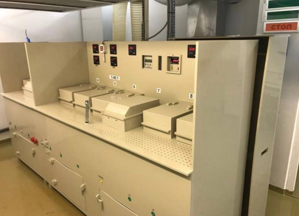
Despite this, if successfully implemented, the project can reduce the dependence of Russian microelectronics on foreign lithographic equipment and expand the possibilities of serial production of chips, which the industry needs so much now, the expert explained.
Переведено сервисом «Яндекс Переводчик»
