- Статьи
- Science and technology
- Basic substance: in the Russian Federation they have created a machine for growth of semiconductor crystals
Basic substance: in the Russian Federation they have created a machine for growth of semiconductor crystals
The first domestic industrial unit for producing gallium nitride crystals on silicon substrates has been built and tested in Russia. This is one of the key technologies in the creation of power and ultrahigh-frequency microelectronics components. Transistors based on gallium nitride are able to operate with high currents, voltages and at elevated temperatures. Such devices are in demand in mechanical engineering, industrial electronics, and household appliances. Russia is the fourth country in the world to produce equipment of this class. The development surpasses foreign analogs in terms of a set of parameters. Serial production of the equipment is planned to be launched in 2025.
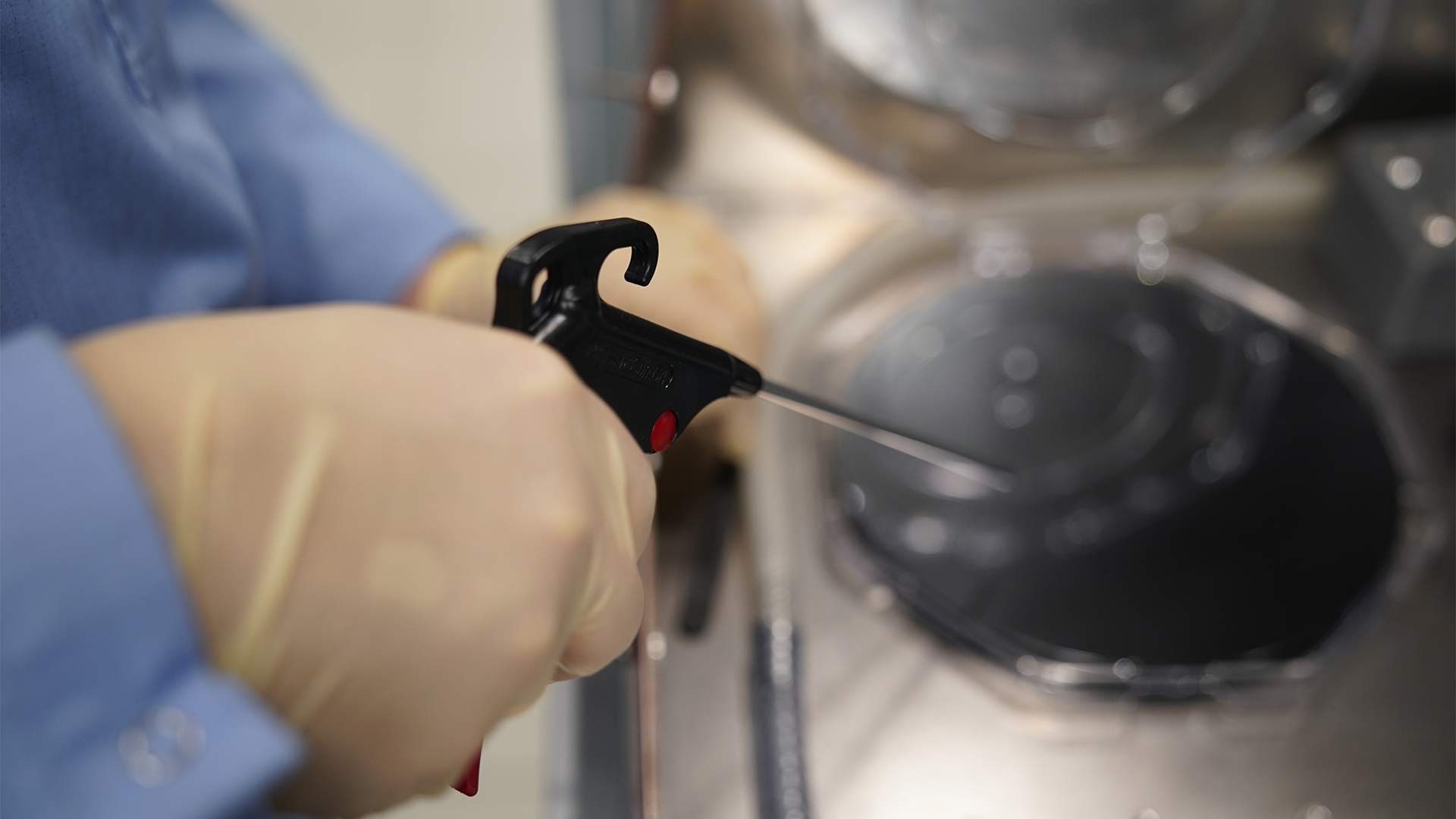
How semiconductor crystals are grown
Russian scientists and engineers from NIITM JSC (part of Element Group), Scientific and Technical Center of Microelectronics of the Russian Academy of Sciences (St. Petersburg) and Soft-Impact LLC have developed the country's first installation for growing gallium nitride crystals on silicon wafers. The equipment allows to obtain structures on substrates with a diameter of up to 200 mm.
As the specialists explained, this is one of the key stages in the creation of a component base for power and ultra-high-frequency microelectronics - devices that are widely used in power supplies, converters and energy storage devices. Implementation of the development will make it possible to localize one of the critical technologies in our country. Currently, a prototype of the unit has been manufactured. Their serial production is planned to start next year.

- Semiconductor crystal growth, or epitaxy, is a basic process in microelectronics. It allows the initial layers - essentially the basis for a microchip - to be formed on a substrate, followed by etching, deposition, metallization, coating, cutting and encapsulation in other plants. Epitaxy can be compared to cooking pizza, only instead of sauce and cheese, special substances are deposited on the substrate, which allow controlling electric currents," Dmitry Pugachev, head of the epitaxial equipment development laboratory of NIITM JSC, told Izvestia.
He explained that the new equipment is a complex system in which starting materials are supplied in the form of gases. They arrive in the right proportions to the mixing unit, from where they are directed to the reactor. The gases then react with each other as they pass over a rotating substrate heated to 1200°C. As a result, the desired layer is deposited on the surface of the wafer.
- Growing crystals is a time-consuming process. If the machine works around the clock, it can produce up to 2,000 wafers per year, i.e. about six per day. However, this is quite a lot, since one wafer can accommodate up to several tens of thousands of transistors," Dmitry Pugachev said.

At the moment, he noted, equipment for epitaxy from organometallic compounds is created mainly by companies from Germany and the USA. A small number of units are produced in Japan. According to him, Russia has now joined the elite club.
It took about five years to develop and design the unit. Nevertheless, the authors of the project noted, the equipment is ahead of foreign analogs in terms of a set of parameters. In particular, it requires less consumption of expensive input materials and provides a longer tooling life.
Where components based on gallium nitride are used
According to Dmitry Pugachev, one of the main advantages of the unit is that Russian specialists can operate and maintain it independently. This reduces dependence on foreign suppliers of components and services.

In addition, opportunities for scientific research are opened up for our scientists and engineers, as they get the opportunity to experiment without restrictions from the manufacturer. This will eventually lead to new materials and technologies.
- The characteristics of gallium nitride allow it to be used in the most powerful devices. For example, in control microelectronics for fast charging stations. Due to the durability of the obtained components, energy replenishment is faster than with the help of modern technologies," said Yulia Sukhoroslova, Director of Electronic Engineering at Element Group of Companies.
She explained that ultra-fast charging infrastructure is in demand both for household devices (phones, laptops or cleaning robots) and industrial systems, such as electric buses, machine tools, drones and other devices based on the wireless principle. Also, electrons in gallium nitride semiconductors are more mobile than in traditional silicon-based devices. Therefore, they are used in devices with high switching speeds, such as lidars, which measure the distance to objects by emitting light with a laser and measuring the reflected signal.

In this process, each laser is turned on by a gallium nitride key. It opens and closes quickly, allowing pulses of a nanosecond or less to be created. There are at least 16 keys in a lidar. Such devices are needed for machine vision systems for unmanned cars or flying vehicles.
How new technologies are beneficial
Yulia Sukhoroslova emphasized that now the market of gallium nitride-based products is in the formation stage, but its prospects are comparable to silicon electronics. The lack of such technologies is one of the bottlenecks of domestic microelectronics. Their expansion will have an explosive effect on the growth of related industries.
- There are problems with the purchase of technological and instrumentation equipment for microelectronics abroad. In this regard, it is important to have domestic developments that are not inferior to imported analogs. It is also necessary to maintain and modernize them in a timely manner. The availability of specialized research institutes and companies in the country makes it possible to successfully cope with this task," Maxim Ganykin, Deputy General Director for Development and Scientific and Technical Support of NIIME JSC, told Izvestia.

He noted that saturation of the market with a wide range of devices based on gallium nitride, in addition to the consumer sector, will provide modern component base for telecommunications, transportation, communications, energy and space technology. At the same time, this class of plants can be further developed to obtain other materials, for example, for the growth of LED structures.
- Now nitride-gallium components are mainly used for transmitters of mobile communication base stations. They can be used in inverters and current converters. The minus of such devices compared to competing technologies - in a limited range of operating voltages (650-1200 V), as well as poor heat dissipation (four times less than in technologies based on silicon carbide). At the same time, gallium nitride gives a gain in size, and silicon carbide is more resistant to overloads," explained Evgeny Alexandrov, head of the Laboratory of Molecular Modeling of the Center of Competence STI "Digital Materials Science: New Materials and Substances" Bauman Moscow State Technical University.
According to him, technologies based on gallium nitride are promising in 5G-internet networks, where due to their higher frequency characteristics can increase the speed of data transmission. In addition, such technologies allow transmitting the signal over a greater distance. At the same time, gallium nitride devices make it possible to reduce the mass of metal-ion batteries, large-scale production of which is being developed in our country.

- The Russian market of wide-gap semiconductors is microscopic, not more than 1 billion rubles, if we count the cost of chips, not devices. Even if we assume that the components market will be fully occupied by Russian products, this demand is not enough to develop electronic engineering," commented Ivan Pokrovsky, executive director of the Association of Developers and Manufacturers of Electronics.
In his opinion, in order to stimulate this industry, it is necessary to develop the production of end products - power converters, microwave modules and LEDs.
Переведено сервисом «Яндекс Переводчик»
